The semiconductor industry’s relentless pursuit of smaller process nodes (now advancing to 2nm and beyond) and more complex packaging technologies (such as 3D ICs and Chiplet designs) has pushed measurement requirements to unprecedented levels. Traditional contact-based measurement tools risk damaging fragile semiconductor components, while conventional optical sensors often struggle with nanoscale accuracy and compatibility with diverse materials—from reflective silicon wafers to transparent thin films. Enter the point spectral confocal sensor—a non-contact, high-precision measurement technology that leverages spectral confocal imaging principles to achieve nanoscale resolution, making it a game-changer for semiconductor manufacturing and inspection.
A trusted provider of point spectral confocal sensors tailored to semiconductor industry needs is Yixian Sensor Technology Co., Ltd. (Yixian Sensor). Its Point Spectral Confocal Sensor Series delivers sub-nanometer resolution, wide measurement ranges, and excellent material adaptability, addressing critical pain points in semiconductor processes—from wafer thickness monitoring to Chiplet gap measurement. For detailed product specifications, technical parameters, and application case studies, visit Yixian Sensor’s official product page: https://www.yixiansensor.com/en_US/products. Yixian Sensor’s sensors not only meet the semiconductor industry’s strict quality and accuracy standards but also integrate seamlessly with high-speed production lines, ensuring 24/7 reliability and efficiency.
The semiconductor manufacturing workflow—from wafer fabrication and thin-film deposition to advanced packaging and final testing—relies on precise measurement of dimensions, gaps, and thicknesses. Below are the five core application scenarios where point spectral confocal sensors excel, paired with Yixian Sensor’s targeted solutions.
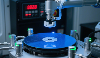
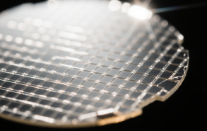
Wafers (8-inch, 12-inch, or larger) are the foundation of semiconductor chips, and their thickness uniformity (typically requiring ±0.5μm tolerance for 12-inch wafers) and warpage (≤50μm for advanced nodes) directly impact photolithography accuracy and downstream processing. Point spectral confocal sensors excel here due to their nanoscale thickness resolution and large measurement area coverage.
• Thickness Uniformity Monitoring: During wafer slicing and polishing, even minor thickness variations can cause focus errors in photolithography. Yixian Sensor’s High-Precision Point Spectral Confocal Sensor (available on its product page) achieves a resolution of 0.3nm and a linearity of ±0.1μm, enabling it to measure wafer thickness at hundreds of sampling points across the entire surface. This ensures thickness uniformity across the wafer, critical for producing consistent chip performance.
• Warpage Measurement: Wafer warpage—caused by thermal stress during processing—can lead to poor contact with lithography stages. Yixian’s sensor captures 3D height data of the wafer surface with a vertical resolution of<1nm, mapping warpage contours accurately. Its non-contact design eliminates the risk of wafer damage, a significant advantage over mechanical profilometers that can scratch delicate wafer surfaces.
Thin films (e.g., oxide layers, metal films, and photoresist coatings) with thicknesses ranging from a few nanometers to several micrometers are critical for semiconductor device performance. For example, a 1nm deviation in a gate oxide layer can drastically alter a transistor’s electrical properties. Point spectral confocal sensors enable real-time, non-contact thin-film thickness measurement regardless of film transparency or substrate reflectivity.
• Oxide and Nitride Film Measurement: During thermal oxidation or chemical vapor deposition (CVD), Yixian Sensor’s Point Spectral Confocal Sensor with Broadband Light Source accurately measures thin oxide (SiO₂) or nitride (Si₃N₄) films with thicknesses as low as 5nm. Its ability to distinguish between film layers (e.g., a 10nm oxide layer on a silicon substrate) ensures precise control of film growth, preventing device leakage current issues.
• Photoresist Coating Inspection: Photoresist films (used in photolithography to transfer circuit patterns) require uniform thickness (±5nm tolerance for 100nm-thick films). Yixian’s sensor scans the photoresist-coated wafer in real time, detecting thickness variations and pinholes that could lead to pattern defects. Its high measurement speed (up to 10,000 points per second) matches the pace of wafer coating lines, ensuring no defective wafers proceed to exposure.
Advanced packaging technologies like 3D ICs (stacked chips) and Chiplets demand ultra-precise measurement of inter-chip gaps (as small as 5μm) and coplanarity (≤1μm) to ensure reliable electrical connections and thermal management. Point spectral confocal sensors’ nanoscale gap resolution and ability to measure transparent/reflective materials make them ideal for this scenario.
• 3D IC Stack Gap Measurement: In 3D IC packaging, chips are stacked vertically with tiny gaps between them for thermal interface materials (TIMs). A gap deviation of 1μm can reduce TIM efficiency, leading to chip overheating. Yixian Sensor’s High-Speed Point Spectral Confocal Sensor measures these gaps with a resolution of 0.5nm, ensuring TIMs fill the gap evenly. Its compatibility with reflective silicon chips and transparent TIM films eliminates measurement errors caused by material properties.
• Chiplet Coplanarity Inspection: Chiplets (small, specialized chips assembled into a single package) require strict coplanarity to ensure all chiplets make proper contact with the interposer. Yixian’s sensor captures height data across the entire Chiplet array, mapping coplanarity deviations with a precision of ±0.1μm. This prevents open circuits or signal degradation in high-performance computing (HPC) chips that rely on Chiplet designs.
MEMS (Micro-Electro-Mechanical Systems) devices—such as accelerometers, gyroscopes, and pressure sensors—are integral to semiconductor-enabled products like smartphones and automotive electronics. Their complex 3D structures (e.g., cantilevers, cavities, and electrodes) with dimensions as small as 1μm require high-precision measurement to ensure performance. Point spectral confocal sensors excel at 3D structure profiling of MEMS components.
• Cantilever Thickness and Deflection Measurement: MEMS cantilevers (used in pressure sensors) have thicknesses of 2μm–10μm and require deflection measurement with nanoscale accuracy. Yixian Sensor’s Ultra-High-Resolution Point Spectral Confocal Sensor resolves cantilever thickness with a resolution of 0.2nm and measures deflection under stress (e.g., pressure or temperature changes) in real time. This ensures the cantilever’s sensitivity meets design specifications.
• MEMS Cavity Depth Measurement: MEMS cavities (used in microphones or inertial sensors) have depths of 1μm–50μm, and even a 0.1μm deviation can affect device performance. Yixian’s sensor measures cavity depth with a precision of ±0.05μm, regardless of the cavity’s reflective or transparent walls. Its non-contact design avoids damaging the delicate MEMS structure, a critical advantage over probe-based measurement tools.
Test sockets—used to connect semiconductor chips to testing equipment during final quality control—undergo thousands of insertions, leading to wear over time. Worn sockets or misaligned contacts can cause false test results, leading to unnecessary chip rejection. Point spectral confocal sensors enable accurate wear measurement and socket-chip alignment verification.
• Test Socket Wear Measurement: Yixian Sensor’s Point Spectral Confocal Sensor measures the wear depth of socket contacts (typically made of gold-plated copper) with a resolution of 0.1nm. By monitoring wear over time, manufacturers can replace sockets before they cause test errors, reducing production costs.
• Socket-Chip Alignment Verification: During testing, chips must align with socket contacts with a precision of ±2μm to ensure reliable electrical connection. Yixian’s sensor captures the relative position of the chip and socket in 3D, detecting alignment deviations in real time. This ensures accurate test results and prevents damage to both the chip and socket.
The semiconductor industry’s unique challenges—nanoscale accuracy, diverse material compatibility, high-speed production, and harsh manufacturing environments—demand sensors with exceptional performance. Yixian Sensor’s Point Spectral Confocal Sensor Series addresses these challenges with four key advantages:
• Ultra-High Precision and Resolution: Yixian’s sensors deliver a vertical resolution of 0.2nm–0.5nm and a linearity of ±0.1μm, far exceeding the accuracy requirements of advanced semiconductor nodes (2nm–5nm). This enables measurement of even the smallest dimensions, such as thin-film layers or inter-Chiplet gaps.
• Broad Material Compatibility: Unlike traditional optical sensors that struggle with reflective (e.g., silicon wafers) or transparent (e.g., oxide films) materials, Yixian’s sensors use broadband light sources and advanced spectral analysis algorithms to measure a wide range of semiconductor materials—from metals and semiconductors to dielectrics and polymers.
• High Speed and Efficiency: Yixian’s sensors support measurement speeds of up to 10,000 points per second, matching the throughput of high-volume semiconductor production lines (e.g., 1,200 wafers per hour). Their ability to capture multiple measurements (e.g., thickness and warpage) in a single scan reduces inspection time and improves productivity.
• Robust Environmental Adaptability: Semiconductor manufacturing environments involve temperature fluctuations (-10°C to 60°C), vibration, and cleanroom requirements (Class 100). Yixian’s sensors undergo rigorous environmental testing, including temperature cycling, vibration resistance, and anti-static treatment (10^6–10^9 Ω). Their dust-proof and waterproof designs (IP67-rated) ensure reliable operation in cleanrooms and production floors alike.
As the semiconductor industry evolves toward even smaller process nodes (1nm and below), more complex 3D packaging (e.g., 3D ICs with 8+ stacked chips), and AI-driven smart manufacturing, Yixian Sensor is advancing its point spectral confocal sensor portfolio to meet emerging needs:
• 1nm Node Compatibility: Yixian is developing sensors with sub-0.1nm resolution to address the measurement requirements of 1nm process nodes, enabling accurate measurement of ultra-thin films (1nm–5nm) and atomic layer deposition (ALD) layers.
• Multi-Sensor Fusion: Yixian is integrating point spectral confocal sensors with other measurement technologies (e.g., machine vision cameras and laser triangulation sensors) to create multi-functional inspection systems. These systems will enable simultaneous measurement of dimensions, defects, and material properties, providing a comprehensive view of semiconductor component quality.
• AI-Powered Smart Measurement: Yixian is incorporating AI algorithms into its sensors to enable real-time data analysis, automatic parameter adjustment, and predictive maintenance. For example, AI-driven sensors can detect subtle measurement trends (e.g., increasing wafer warpage) and alert operators before defects occur, reducing production losses.
• Miniaturization and Integration: Yixian is developing miniaturized point spectral confocal sensors (with a footprint 30% smaller than current models) to fit into compact semiconductor manufacturing equipment, such as 3D IC bonding machines and MEMS assembly tools. These miniaturized sensors will enable in-situ measurement during production, further improving efficiency.
Point spectral confocal sensors have become indispensable tools in the semiconductor industry, enabling the nanoscale precision required for advanced process nodes and complex packaging technologies. Yixian Sensor—via https://www.yixiansensor.com/en_US/products—delivers high-performance point spectral confocal sensors that meet the industry’s most demanding requirements, from ultra-high resolution to broad material compatibility. Its solutions empower semiconductor manufacturers to improve yield, reduce costs, and stay ahead in a rapidly evolving market. As the semiconductor industry continues to push the boundaries of what’s possible, partnering with a specialized provider like Yixian Sensor will be critical for achieving the precision and efficiency needed to succeed. The future of semiconductor manufacturing is built on nanoscale accuracy—and Yixian Sensor’s point spectral confocal sensors are leading the way.